The chips in our devices are powered by transistors and integrated circuits so small that they can barely be detected by our most advanced imaging techniques. How chip makers manage to do quality control when they can’t even see what they’re working on is a really good question. But a new method from Swiss researchers provides an incredibly detailed look at details on the level of nanometers — and in 3D, to boot.
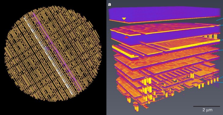
That entire circle in the image above? 10 micrometers wide. Impressive, right?
Normally in a post like this, I, the well-informed tech writer, would try to walk you, the poor benighted reader, though the technology step by step. But I’ve got to be honest with you: This time I’m as lost as the next guy. So let’s try to work through it together. Sayeth mine authors at the Paul Scherrer Institut:
Modern X-ray optics paired with synchrotron light sources have changed the landscape, with Fresnel zone plates and Kirkpatrick-Baez mirror pairs producing small (7 nm in diameter at 20 keV; ref. 15), intense beams which could be used for scanning probe microscopy.
Kirkpatrick and Baez invented the X-ray microscope in the 1940s, but it and fresnel stuff have come a long way. Synchrotrons create super-precise light beams. So basically this is not an entirely new concept, but technological limitations have prevented it from being used this way before.
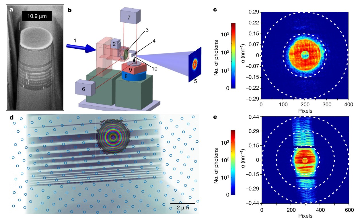
Self-explanatory, right? The synchrotron sends the X-rays through the lens array, through the sample and onto the detector. The dots are the locations of individual scans as the sample is spun around.
Okay, next:
Highly coherent radiation produced by undulators at third-generation X-ray synchrotrons has allowed the development of a mixed real-space/reciprocal-space imaging technique, called ptychographic X-ray computed tomography (PXCT).
Real-space scanning would be like getting an X-ray of your arm, where you record the signal strength on the other side; different substances absorb different amounts and frequencies of the radiation. Reciprocal space has to do with the… well, it’s kind of like a quantum shadow that can tell you about the makeup of an atomic lattice.
This video explains it, kind of:
Still with me? Then we’ll move on:
Here the speckle pattern (in reciprocal space), due to density fluctuations in the sample, from a bounded beam illuminating the sample is measured as a function of rotation and translation (in real space) of the sample. The set of patterns can then be transformed via iterative reconstruction algorithms into a full 3D real-space image of the density variations in the sample…
In this case the subject is too small to read like a real-space X-ray, so they have to rely on reciprocal-space imagery — but you still need real-space measurements to contextualize it. Because it records density, it can determine areas of greater or lesser density, it can discern between the likes of conductors, substrates and empty space.
…with a resolution given not by the step and beam size, as in scanning probe microscopy, but by the noise level of the features which are outermost in the speckle patterns, that is, representing the shortest length density fluctuations.
So by tracking the reciprocal lattice pattern generated and mathematically tying it to the real-world positioning of the chip, they can reconstruct it into a 3D model. And because details are generated at the level of the shadows cast by the atoms in the path of the beam, not by the much larger beam itself, it’s much higher resolution than previous X-ray techniques.
Okay, that wasn’t so bad, was it? And here’s the result:
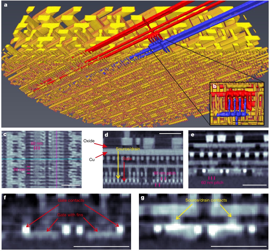
The 3D rendering at top is formed by analyzing various close-ups and angles. You can see individual gates at the bottom. The scale bars are 500 nanometers, so you’re seeing details much smaller than that.
A setup like this means that chips can be scanned both by their creators and competitors at a level that reveals pretty much every transistor. So long, trade secrets!
Actually it would take a very long time to image an entire chip this way, but it will be very useful for testing whether new chip designs (which are getting thicker and more interconnected) are being laid down properly, or whether a secretive chip company is really using some rumored technology or fabrication process.
The paper describing the technique was published today in Nature.